- 您现在的位置:买卖IC网 > Sheet目录1992 > CY284108ZXC (Silicon Laboratories Inc)IC CLOCK SERV CK410B 56TSSOP
CY284108
........................ Document #: 38-07713 Rev. *B Page 2 of 16
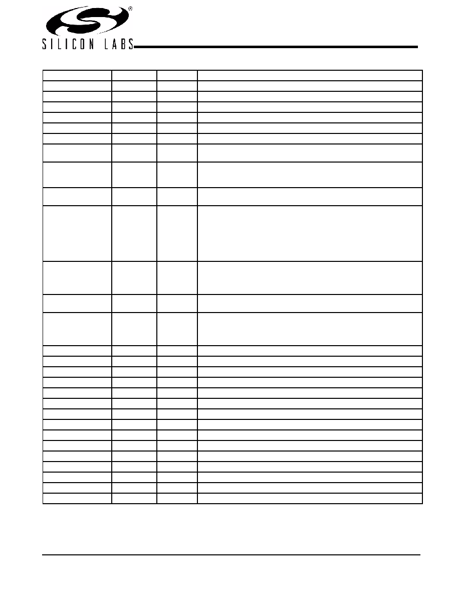
Pin Description
Name
Pin Number
Type
Description
X1
52
I
14.18 MHz crystal input
X2
51
O, SE
14.18 MHz crystal output
REF[1:0]
55, 54
O, SE
14.18 MHz reference clock
PCI[3:0]
6,5,4,3
O, SE
33 MHz clocks
PCIF[2:0]
11,10,9
O,SE
33 MHz free running clock. Is not disabled via Software PCI_STOP.
USB_48
13
O, SE
Fixed 48 MHz USB clock output
CPU[T/C][3:0]
37,36;40,39;
43,42;46,45
O, DIF
Differential CPU clock outputs
SRC[T/C][4:0]
26,27;24,23;
21,22;19,18;
16,17
O, DIF
Differential serial reference clocks. SRC[T/C]4 is recommended for SATA.
FS_A
48
I
3.3V-tolerant input for CPU frequency selection. Refer to DC Electrical
Specifications table for Vil_FS and Vih_FS specifications.
FS_B/TEST_MODE
49
I
3.3V-tolerant inputs for CPU frequency selection/selects REF/N or Hi-Z
when in test mode. Refer to DC Electrical Specifications table for Vil_FS and
Vih_FS specifications.
At VTTPWRGD# asserted low (see page 10 for diagram), this pin is sampled
to determine test mode functionality
0 = Hi-Z
1 = REF/N
FS_C/TEST_SEL
56
I
3.3V-tolerant inputs for CPU frequency selection/selects test mode if pulled
to 3.3V when VTT_PWRGD# is asserted low (seepage 10 for diagram).
Refer to DC Electrical Specifications table for Vil_FS and Vih_FS specifica-
tions
IREF
33
I
A precision resistor is attached to this pin, which is connected to the internal
current reference
VTT_PWRGD#/PD
31
I, PD
DF3.3V LVTTL input is a level sensitive strobe used to latch the FS_A,
FS_B, FS_C/TEST_SEL inputs. After VTT_PWRGD# (active low) assertion,
this pin becomes a realtime input for asserting power down (active high).
See page 10 for diagram.
SCLK
29
I
SMBus-compatible SCLOCK
SDATA
30
I/O
SMBus-compatible SDATA
VDD_REF
53
PWR
3.3V power supply for outputs
VSS_REF
50
GND
Ground for outputs
VDD_PCI
1,8
PWR
3.3V power supply for outputs
VSS_PCI
2,7
GND
Ground for outputs
VDD_48
12
PWR
3.3V power supply for outputs
VSS_48
14
GND
Differential CPU clock outputs
VDD_SRC
15,25,28
PWR
3.3V power supply for outputs
VSS_SRC
20
GND
Ground for outputs
VDD_CPU
38,44,47
PWR
3.3V power supply for outputs
VSS_CPU
41
GND
Ground for outputs
VDD_A
35
PWR
3.3V power supply for outputs
VSS_A
34
GND
Ground for outputs
NC
32
–
No Connection
发布紧急采购,3分钟左右您将得到回复。
相关PDF资料
CY28410OXC-2
IC CLOCK CK410 GRANTSDALE 56SSOP
CY28410OXC
IC CLOCK CK410 GRANTSDALE 56SSOP
CY28411ZXC
IC CLOCK CK410M ALVISO 56TSSOP
CY28442ZXC-2
IC CLOCK ALVISO PENTM 56TSSOP
CY28445LFXC-5
IC CLOCK CALISTOGA CK410M 68QFN
CY28446LFXC
IC CLOCK CALISTOGA CK410M 64QFN
CY28447LFXC
IC CLOCK CALISTOGA CK410M 72QFN
CY28547LFXCT
IC CLOCK CK505/410M INTEL 72QFN
相关代理商/技术参数
CY284108ZXCT
功能描述:时钟发生器及支持产品 Server, CK410B RoHS:否 制造商:Silicon Labs 类型:Clock Generators 最大输入频率:14.318 MHz 最大输出频率:166 MHz 输出端数量:16 占空比 - 最大:55 % 工作电源电压:3.3 V 工作电源电流:1 mA 最大工作温度:+ 85 C 安装风格:SMD/SMT 封装 / 箱体:QFN-56
CY28410OC
制造商:SPECTRALINEAR 制造商全称:SPECTRALINEAR 功能描述:Clock Generator for Intel Grantsdale Chipset
CY28410OCT
制造商:SPECTRALINEAR 制造商全称:SPECTRALINEAR 功能描述:Clock Generator for Intel Grantsdale Chipset
CY28410OXC
功能描述:时钟发生器及支持产品 SysClk Intel Lakeprt & Grantsdale Chipset RoHS:否 制造商:Silicon Labs 类型:Clock Generators 最大输入频率:14.318 MHz 最大输出频率:166 MHz 输出端数量:16 占空比 - 最大:55 % 工作电源电压:3.3 V 工作电源电流:1 mA 最大工作温度:+ 85 C 安装风格:SMD/SMT 封装 / 箱体:QFN-56
CY28410OXC-2
功能描述:时钟发生器及支持产品 SysClk Intel Lakeprt & Grantsdale Chipset RoHS:否 制造商:Silicon Labs 类型:Clock Generators 最大输入频率:14.318 MHz 最大输出频率:166 MHz 输出端数量:16 占空比 - 最大:55 % 工作电源电压:3.3 V 工作电源电流:1 mA 最大工作温度:+ 85 C 安装风格:SMD/SMT 封装 / 箱体:QFN-56
CY28410OXC-2T
功能描述:时钟发生器及支持产品 SysClk Intel Lakeprt & Grantsdale Chipset RoHS:否 制造商:Silicon Labs 类型:Clock Generators 最大输入频率:14.318 MHz 最大输出频率:166 MHz 输出端数量:16 占空比 - 最大:55 % 工作电源电压:3.3 V 工作电源电流:1 mA 最大工作温度:+ 85 C 安装风格:SMD/SMT 封装 / 箱体:QFN-56
CY28410OXCT
功能描述:时钟发生器及支持产品 SysClk Intel Lakeprt & Grantsdale Chipset RoHS:否 制造商:Silicon Labs 类型:Clock Generators 最大输入频率:14.318 MHz 最大输出频率:166 MHz 输出端数量:16 占空比 - 最大:55 % 工作电源电压:3.3 V 工作电源电流:1 mA 最大工作温度:+ 85 C 安装风格:SMD/SMT 封装 / 箱体:QFN-56
CY28410ZC
制造商:SPECTRALINEAR 制造商全称:SPECTRALINEAR 功能描述:Clock Generator for Intel Grantsdale Chipset